Plasma-Enhanced CVD from TEOS and Oxygen
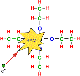
Combining TEOS with ozone, in an attempt to preserve the excellent step coverage of TEOS/oxygen LPCVD at lower temperatures, was successful but as we noted, results in significant problems with film stress, moisture absorption, and stability not observed by most other techniques. Another approach to achieving deposition from TEOS at lower temperatures is to add plasma excitation.
Plasma-enhanced deposition of oxides from TEOS (PETEOS) was first reported in the late 60's. Extensive commercial development was performed in the 80's. Commercial processes employ parallel-plate showerhead reactors with RF plasma excitation, typically operating at pressures of 1 to 10 Torr, with gas flows of a few slpm including a few 10's to hundreds of sccm of TEOS. Bubblers or liquid injection is employed to deliver the TEOS, as in thermal CVD.

Film Properties
With plasma excitation, high deposition rates are obtained at temperatures of 300-450 °C from TEOS / oxygen. In single-wafer reactors rates of 5000-10,000 Å/min can be achieved, using pressures around 6-10 Torr and very small electrode gaps (<6 mm). The problems encountered in thermal TEOS/ozone deposition (water absorption, silanol, stress, cracking) are also present in plasma-deposited films, but the availability of the plasma allows improved flexibility in dealing with them. Increasing RF power and increasing pressure while decreasing electrode gap, and increasing the oxygen:TEOS ratio, all help produce films which are "dry" and stable in air. Increasing the pressure with corresponding decreases in the gap has the nice property of increased rate without degraded stability. However, increasing the amount of oxygen decreases the deposition rate, so the final process is a tradeoff of stability with throughput. The use of dual-frequency reactors is effective in adjusting stress from tensile to compressive with little effect on other parameters.
Conformality is greatly superior to that obtained from plasma or thermal silane/oxygen deposition, but inferior to thermal TEOS. "Vertical" deposition, presumably from ionized species, plays a significant role in the total deposition rate. It has been reported that dual-frequency processes achieve better conformality than single-frequency processes. By alternately depositing oxide with PETEOS process, and subjecting the wafer to a sputter etching step (in a separate chamber) which removed the overhanging corners, excellent gap fill may be obtained but at a significant cost in throughput: this is the "dep-etch" process commercialized by Applied Materials in the late 80's. Due to the use of magnetized plasmas for sputter etch, this process also encountered some problems with plasma damage of underlying transistors. Plasma TEOS films have also been observed to display large fixed charge densities, particularly if deposited under conditions producing compressive stress, after high-temperature annealing.
Plasma TEOS films are often used to encapsulate thermal TEOS-ozone oxide or spin-on glass, to protect it from ambient moisture. A PETEOS underlayer has better step coverage ability than plasma-enhanced silane films, so the thermal or SOG oxide has an easier task filling trenches or holes with a PETEOS underlayer. However, PETEOS is a relatively poor moisture barrier, and thus conformality and reliability impact must be balanced.
References:
"Plasma TEOS Process for Interlayer Dielectric Applications" B. Chin, E. Van de Ven Solid State Technology April 1988 p. 119
"Plasma TEOS as in Intermetal Dielectric In Two Level Metal Technology" G. Hills, A. Harrus and M. Thoma, Solid State Technology, April, 1990 p. 127
"Characterization of a multiple-step in situ plasma enhanced chemical vapor deposition (PECVD) tetraethylorthosilicate (TEOS) planarization scheme for submicron manufacturing" J. Perchard, H. Smith, R. O'Connor, J. Olsen and K. Law, SPIE Proceedings vol. 1188 Multichamber and Insitu Processing of Electronic Materials (1989) p. 75
"Reaction Mechanisms of Plasma- and Thermal-Assisted Chemical Vapor Deposition of Tetraethylorthosilicate Oxide Films" S. Nguyen, D. Dobuzinsky, D. Harmon, R. Gleason and S. Fridmann [IBM] J. Electrochem. Soc. 137 2209 (1990)
"A Characterization of PECVD TEOS BPSG Planarity and Metal-Field Vt on a Submicron CMOS EPROM" E. Ibok, S. Garg, E. Lee, J. O'Banon, VMIC 1991 p. 369
"Stress in SiO2 Films Deposited by Plasma and Ozone Tetraethylorthosilicate Chemical Vapor Deposition Processes" K. Ramkumar and A. Saxena,J. Electrochem. Soc. 139 1437 (1992)
"Characterization of TEOS oxides used in the isolation module of high-speed bipolar and BiCMOS circuits" S. Wilson and H.-B. Liang, Thin Solid Films 220 59 (1992)
"Modeling of PECVD TEOS Oxide Step Coverage Using an Overhang Structure" C. Chang, J. McVittie, K. Saraswat, Proc. 9th Symposium Plasma Processing (1992) ed. G. Mathad, D. Hess [Electrochemical Society]
"Electrical Characterization of Doped and Undoped PECVD TEOS Oxides" J. Butler, G. Allen, A. Hall, R. Nowak, VMIC Conference, June 12-13, 1990 p. 387
"Elimination of in-process multilevel interconnect stress voids through optimization of plasma enhanced chemical vapor deposition parameters" G. Grivna, C. Leathersich, H. Shin and W. Cowden J. Vac. Sci. Technol. B11 55 (1993)
"Relationship between Water Diffusivity of Dielectric Films and Accelerated Hot Carrier Degradation Caused by Water" K. Fukuda, T. Nakano, M. Fujishima, N. Mura, K. Tokunaga, A. Tsuzumitani and S. Ichinose [Kawasaki Steel] Jpn. J. Appl. Phys. 34 963 (1995)
"Optimization of intermetal dielectric deposition module using simulation" J. Li, J. McVittie, J. Ferziger and K. Saraswat , J. Vac. Sci. Technol. B13 1867 (1995)
"Enhanced Hot-Carrier Degradation Due to Water-Related Species in Plasma-Enhanced Tetraethoxysilane Oxide" T. Yamaha, Y. Inoue, T. Fujioka, O. Hanagasaki, and T. Hotta [Yamaha] J. Electrochem. Soc. 142 2743 (1995)
"Process Induced Gate Oxide Damage Issues in Advanced Plasma Chemical Vapor Deposition Processes", D. Cote, S. Nguyen, V. McGahay, C. Waskiewicz, S. Chang, A. Stamper, P. Weigand, N. Shoda and T. Matsuda, First International Symposium on Plasma Process-Induced Damage, May 13-14 1996, Santa Clara, CA p. 61
Return to Tutorial Table of Contents
Book version of the CVD Tutorial
